Характеристики
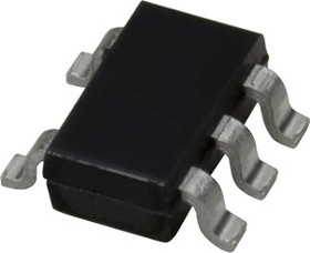
SN74LVC1G126DBVR, Одиночный шинный буфер с тремя состояниями …The SN74LVC1G126DBVR is a single Bus Buffer Gate designed for 1.65 to 3.6V VCC operation. The LVC1G126 device is a single line driver with 3-state output. The output is disabled when the output-enable input is low. The device contains a dual buffer gate with output enable control and performs the Boolean function Y = A. This device is fully specified for partial-power-down applications using IOFF. The IOFF circuitry disables the outputs, preventing damaging current backflow through the device when it is powered down. To ensure the high-impedance state during power up or power down, OE should be tied to GND through a pull-down resistor and the minimum value of the resistor is determined by the current-sourcing capability of the driver.
• Provides down translation to VCC
• IOFF Supports live insertion, partial-power-down mode and back drive protection
• Latch-up performance exceeds 100mA per JESD 78, class II
• Inputs accept voltages to 5.5V
• 3.7ns at 3.3V Propagation delay (tpd)
• 10µA ICC Low power consumption
• ±24mA Output drive at 3.3V
• Green product and no Sb/Br
 Личный кабинет


 Загрузка