Характеристики
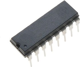
CD4042BE, Триггер D-типа х 4 (=КР1561ТМ3) [PDIP-16]The CD4042BE is a CMOS Quad-clocked ‘D’ Latch, each strobed by a common clock. Complementary buffered outputs are available from each circuit. The impedance of the n and p-channel output devices is balanced and all outputs are electrically identical. Information present at the data input is transferred to outputs Q and Q during the CLOCK level which is programmed by the POLARITY input. For POLARITY=0 the transfer occurs during the 0 CLOCK level and for POLARITY=1 the transfer occurs during the 1 CLOCK level. The outputs follow the data input providing the CLOCK and POLARITY levels defined above are present. When a CLOCK transition occurs (positive for POLARITY=0 and negative for POLARITY=1) the information present at the input during the CLOCK transition is retained at the output until an opposite CLOCK transition occurs.
• Clock polarity control
• Q and Q outputs
• Common clock
• Low power TTL compatible
• Standardized, symmetrical output characteristics
• 100% Tested for quiescent current at 20V
 Личный кабинет


 Загрузка