Характеристики
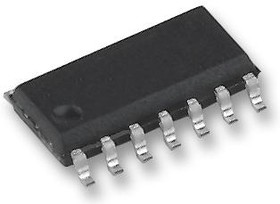
SN74LVC74AD, Триггер D-типа с сбросом и предустановкой …The SN74LVC74AD is a dual positive-edge-triggered D-type Flip-flop designed for 1.65 to 3.6V VCC operation. A low level at the preset (PRE) or clear (CLR) inputs sets or resets the outputs, regardless of the levels of the other inputs. When PRE and CLR are inactive (high), data at the data (D) input meeting the setup time requirements is transferred to the outputs on the positive-going edge of the clock pulse. Clock triggering occurs at a voltage level and is not directly related to the rise time of the clock pulse. Following the hold-time interval, data at the D input can be changed without affecting the levels at the outputs. The data I/Os and control inputs are overvoltage tolerant. This feature allows the use of these devices for down-translation in a mixed-voltage environment.
• Maximum tpd of 5.2ns at 3.3V
• Latch-up performance exceeds 250mA per JESD 17
• Green product and no Sb/Br
 Личный кабинет


 Загрузка