Характеристики
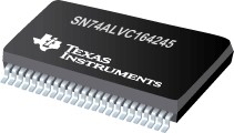
SN74ALVC164245DGGR, Преобразователь логического уровня [TSSOP-48]The SN74ALVC164245DGGR is a 16-bit non-inverting 2.5 to 3.3 or 3.3 to 5V level shifting Bus Transceiver with three-state outputs. The SN74ALVC164245 is designed for asynchronous communication between data buses. The control circuitry is powered by VCCA. To ensure the high-impedance state during power up or power down, the output-enable (OE) or input should be tied to VCC through a pull up resistor, the minimum value of the resistor is determined by the current-sinking capability of the driver. The logic levels of the direction-control (DIR) input and the output-enable (OE) or input activate either the B-port outputs or the A-port outputs or place both output ports into the high-impedance mode. The device transmits data from the A-bus to the B-bus when the B-port outputs are activated and from the B-bus to the A-bus when the A-port outputs are activated.
• Maximum TPD of 5.8ns at 3.3V
• ±24mA Output drive at 3.3V
• Control inputs VIH/VIL levels are referenced to VCCA voltage
• Latch-up performance exceeds 250mA per JESD 17
• Green product and no Sb/Br
 Личный кабинет


 Загрузка