Характеристики
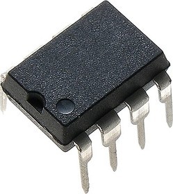
TLC277CP, Операционный усилитель, двухканальный, 2.2МГц [DIP8]The TLC277CP is a dual precision Operational Amplifier combines a wide range of input offset voltage grades with low offset voltage drift, high input impedance, low noise and speeds approaching those of general-purpose BiFET device. This device uses Texas Instruments silicon-gate LinCMOS™ technology, which provides offset voltage stability far exceeding the stability available with conventional metal-gate processes. The extremely high input impedance, low bias currents and high slew rates make this device ideal for applications previously reserved for BiFET and NFET products. These advantages, in combination with good common-mode rejection and supply voltage rejection, make this device a good choice for new state-of-the-art designs as well as for upgrading existing designs. In general, many features associated with bipolar technology are available on LinCMOS™ operational amplifier without the power penalties of bipolar technology.
• Single-supply operation
• Common-mode input voltage range extends below the negative rail
• Output voltage range includes negative rail
• ESD-protection circuitry
• Designed-in latch-up immunity
• Input offset voltage drift — Typically 0.1µV/month, including the first 30 days
• 500µV at 25°C, VDD=5V Maximum trimmed offset voltage
• 25nV/√Hz at f=1kHz Typically low noise
• 10¹² Typical high input impedance
 Личный кабинет


 Загрузка